Sign up today and we»ll send you a 10% discount code towards your first purchase. Some restrictions apply.
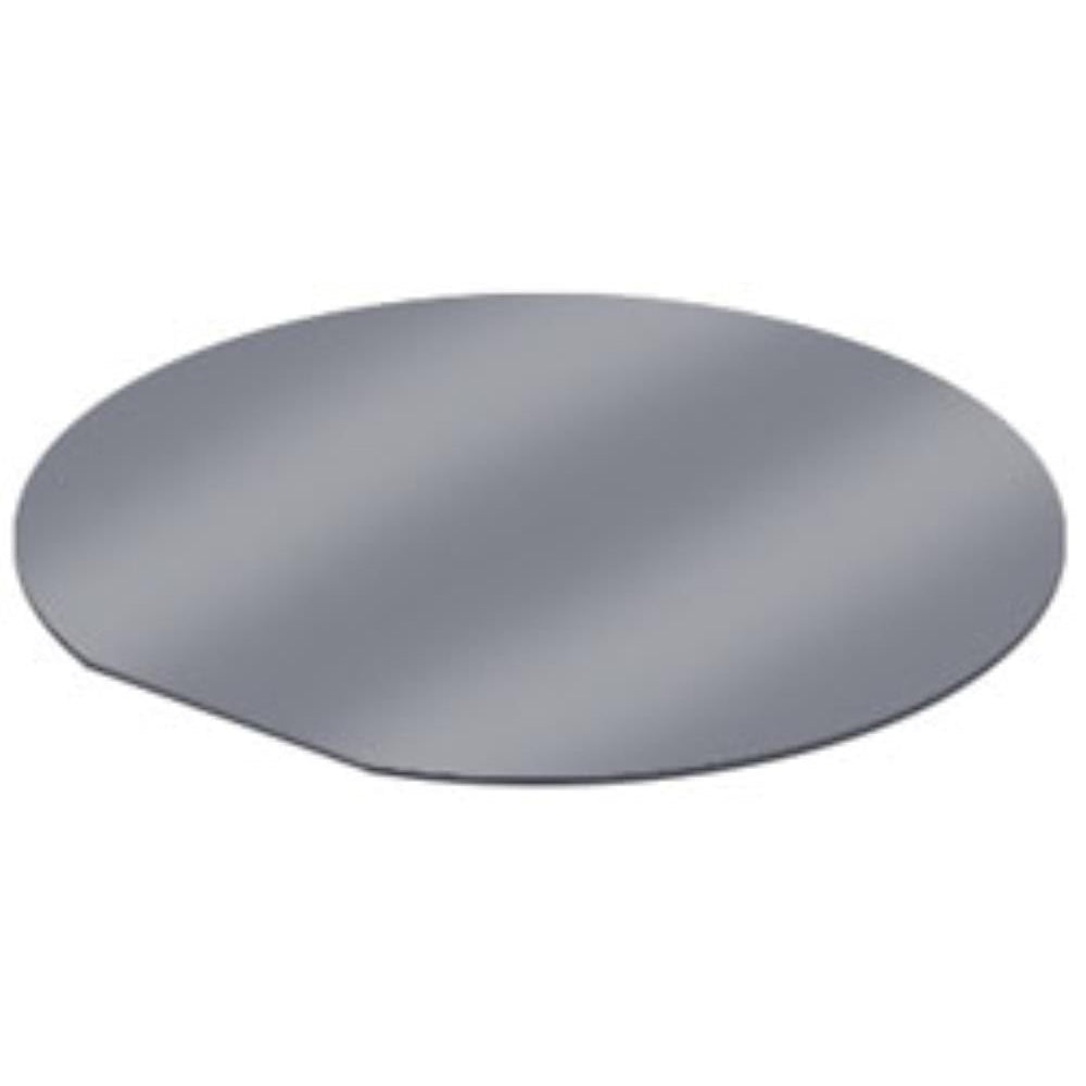
Ultra-Flat silicon wafer for demanding substrate studies. Can also be used as substrate for AFM or SEM samples by dicing the wafer into smaller pieces using a scriber and the Wafer Cleaving / Glass Breaking Pliers. The ultra-flat silicon wafer is shipped in a wafer carrier.
Properties for 150mm ultra-flat wafer:
- Orientation: <,100>,
- Grade: Prime / CZ Virgin
- Resistivity: 1-10 Ohm/cm
- Type: P / Dopant: Boron
- Wafer Thickness: 675 +/- 25um
- TTV: <,= 1.5um
- Warp: <,=30um / Bow: <,= 30um
Particles: <,= 30@>,=0.2um - Front surface: Polished
- Back Surface: Etched
- Flat: 1 per SEMI Standard (flat length 57.5 ±2.5mm)
- Roughness: Typical 2-3
Технические характеристики
GASUF06