Sign up today and we»ll send you a 10% discount code towards your first purchase. Some restrictions apply.
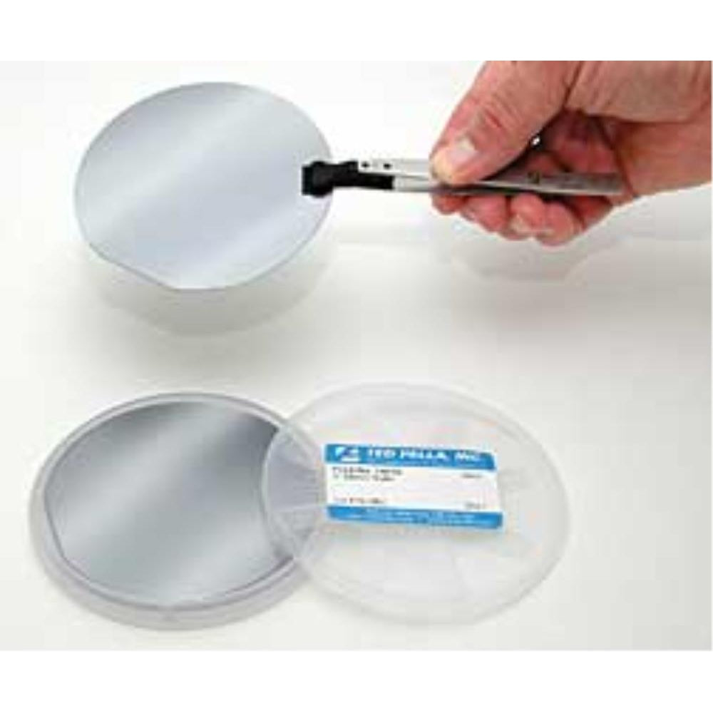
These silicon wafers can be used either as a substrate for thin film research or to make small silicon substrates by dicing the wafer into smaller pieces using a scriber and the Wafer Cleaving / Glass Breaking Pliers. The wafer is shipped in a wafer carrier.
Properties:
- Orientation: <,100>, or <,111>, for 3″ (76.2mm) wafer
- Resistance: 1-30 Ohms
- Type P: (Boron) (1 primary flat)
- No SiO2 top coating
- Wafer thickness:
- 25.4mm diameter = 10 — 12 mill (254 — 304µm)
- 50.8mm diameter = 9 — 13 mill (230-330um)
- 76.2mm diameter = 13.6 — 18.5 mill (345-470um)
- 101.6mm diameter = 18.7 — 22.6 mill (475-575um)
- 127mm diameter = 23.6 — 25.2 mill (600-690um)
- Roughness: 2nm
- TTV: = <,20um
- Wafer is polished on one side
Технические характеристики
GAS02